I thought this video was worth posting because I am having a very difficult time finding automotive manufacturing content from Japanese companies. I know many auto firms cooperate with Japanese companies, but it appears they keep their information out of the public arena. From what I have seen, Europeans seem to be the least concerned with letting insiders into their plants and the Japanese seem the be the most elusive.
This video is completely in Japanese and is well over 10 years old, but it is still interesting to see how the Nissan 180SX (S13 chassis) was manufactured. Production for the car began in 1989 and ended in 1998. If I had to guess, this video is probably from the early 90's. As you watch the video note that virtually everything is performed manually by the production workers including welding and glue application/window placement.
Showing posts with label Video Tour. Show all posts
Showing posts with label Video Tour. Show all posts
Saturday, November 17, 2007
Cutting Edge: Intel's Fab 32 (Arizona)
Intel's Fab 32 is a Cutting Edge $3 Billion Dollar, 300mm Fab with a 45nm process that will go into production in the second half of 2007 (Now!). Intel's Press Release and video tell you almost everything you need to know:
"When completed, Fab 32 will become Intel's sixth 300-mm wafer facility. The structure will be about 1 million square feet with 184,000 square feet of clean room space. The project will create up to 1000 new Intel jobs at the Arizona site over the next several years. During the construction phase, more than 3,000 skilled trades people will be hired to work on the project.
Intel currently operates four 300-mm fabs that provide the equivalent manufacturing capacity of about eight 200-mm factories. Those factories are located in Oregon, Ireland and New Mexico. The company also has an additional 300 mm fab currently under construction in Arizona (Fab 12) scheduled to begin operations later this year, and one expansion in Ireland (Fab 24-2) scheduled to begin operations in the first quarter of next year.Manufacturing with 300-mm wafers (about 12 inches in diameter) dramatically increases the ability to produce semiconductors at a lower cost compared with more widely used 200-mm (eight-inch) wafers. The total silicon surface area of a 300-mm wafer is 225 percent, or more than twice that of a 200-mm wafer, and the number of printed die (individual computer chips) is increased to 240 percent. The bigger wafers lower the production cost per chip while diminishing overall use of resources. Three-hundred-mm wafer manufacturing will use 40 percent less energy and water per chip than a 200-mm wafer factory."
Friday, November 9, 2007
Direct from Dell.... (Austin, TX)
Dell has a very fascinating history, business model, and supply chain strategy and the company is well known in the computer arena. Dell has had suffered from some issues over the last few years, but overall the company's operations are solid. This Dell Plant Tour Video is a little dated, but it is still very interesting to see the general framework at the Dell factory.
I happen to have studied Dell very closely since about 2001, and I was lucky enough to attend many presentations by Dell employees (and even know several). A few things to note are that as of 2004-2006 Dell operated under the following structure:
I happen to have studied Dell very closely since about 2001, and I was lucky enough to attend many presentations by Dell employees (and even know several). A few things to note are that as of 2004-2006 Dell operated under the following structure:
- Laptops are made overseas (generally in Taiwain) by ODMs and air freighted to the US. This likely is due to labor savings and the density to price ratio.
- Dell's Topfer Manufacturing Center in Austin, TX (TMC is building PN2) assembles Desktop PCs while the building next door (PN1) builds servers.
Additionally, since this video was made many changes have been implemented at TMC:
- Barcode scanning has been changed to RFID on the totes that move around the factory.
- Inventory is kept low because Dell does not keep a component inventory warehouse themselves. Their components are kept at consignment warehouses next door where the suppliers own the inventory until it is pulled for a customer order.
- The Boxing line is still performed manually in some instances, but for certain platforms the High Velocity Kitting line completes the process via automation.
Thursday, November 8, 2007
Facility Showcase: BMW Leipzig
BMW has a short yet detailed video on their facility in Leipzig, Germany. It discusses the thought process that went into deciding facility attributes, and also provides some insight into BMW as a whole. The robotics in the body shop, paint shop, welding, etc. are amazing to watch, and the facility layout is also quite impressive. From what I can tell there are few if any paper travelers at Leipzig, and the operation itself appears world class.
Wednesday, November 7, 2007
Maserati: Italian Luxury
 Maserati has an interesting history with ownership changing many times over the years. Within approximately the last decade, Maserati has gone from Fiat ownership, to join Fiat/Ferrari ownership, to full Ferrari ownership, back to full Fiat ownership (which is even more interesting since Fiat owns Ferrari). Over this period Ferrari helped reinvigorate Maserati and even developed the engine and drivetrain which is shared amongst the different models.
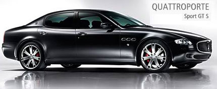 Maserati's plant tour shows some great examples of component commonality because their lineup appears to have many common parts with different exterior styling to address very specific customer segments.
- Quattroporte - Four Door sedan (Quattroporte means four doors in Italian)
- GranTurismo - Hard Top Coupe (2+2)
- GranSport - Hard Top Coupe (2+2)
- Gransport Spyder - Two Seat Convertible; No back seat
- Coupe - Hardtop Coupe (2+2)
In fact, per the video the only difference between the the Quattroporte and Granturismo is that the Quattroporte has a larger grille. Maserati only manufactures ~7,000-10,000 vehicles per year, but would like to increase that number as sales in North America increase.
Some interesting points from the Maserati Plant Tour video that I noted as I watched it were that:
- Maserati has implemented a JIT methodology, and looked to have much of their information on the Paper travelers that move with each car.
- Around the 3 minute mark the spokeswoman notes that the vehicle being shown is definitively an american car because of the cup holders!
- Engines are tested as modules by Ferrari and also Final Tested in a finished car up to 250 kpm. Each car is then driven 80km over city streets, mountain roads, and highways.
- If you pick up your car at the Maserati showroom you will find your car covered with a blue cover so you can unveil your car, open your champagne, and party with Maserati! You also get your own photographer so you can be assurred the event is documented. Note: Sounds very similiar to Ferrari to me!
Thursday, October 25, 2007
Canon Lens Plant Tour
I don't know as much about it, but optics are also an area I find very interesting. I took Engineering Physics in college and have since forgotten much of it, but I have a great appreciation for the engineering that goes into anything dealing with light and also sound. While looking for lens information I found someone who stated that he "believes Canon is the only camera company that manufactures all their own lens elements from raw materials (at their Utsunomiya plant). Leica makes lenses too, but they also OEM out some of their lenses entirely."
This Canon plant tour shows all of the steps to create a camera lens from start to finish, and the featured product the EF 500mm F4L IS USM is a gigantic lens at 19.7 inches in length! Also be sure to check out the Lens Gallery at the bottom which has more information about lens materials and physics.
This Canon plant tour shows all of the steps to create a camera lens from start to finish, and the featured product the EF 500mm F4L IS USM is a gigantic lens at 19.7 inches in length! Also be sure to check out the Lens Gallery at the bottom which has more information about lens materials and physics.
Tuesday, October 23, 2007
Gigabyte Plant Tour
 Today's Plant tour is of the Gigabyte Nan-Ping Factory in Taiwan. To provide some background, GIGABYTE, which was founded in 1986, has become one of the world's largest motherboard manufacturers. In addition to motherboards, GIGABYTE has further expanded its product portfolio to include graphics cards, notebook and desktop PCs, digital home entertainment appliances, networking servers, and other electronic products.
Gigabyte allowed several sites to provide plant tour coverage, so there is both a short, 2 minute video made by Firing Squad (2006), and detailed virtual tour with commentary from PCStats (2005). The factory assembles both motherboards and graphics cards, and is a great primer for those who have never looked at the detailed steps involved in making today's latest electronics. Many people do not realize that the whole process of manufacturing PCBs and similiar devices is very manual labor intesive, and therefore is almost always performed offshore from the US.
"Without a doubt, motherboards are the most complex and essential part of the
modern PC. Not only do they hold the chipsets that pass data from peripherals,
drives and memory to the processor, they also provide slots and ports for all
your other system components and the circuits through which all data must pass.
Perhaps surprisingly then, motherboards get very little respect in the computing
press as compared to other components. They are perpetually the team player and
not the star of the show, and are generally priced as such.With this in mind, it's surprising to learn the amount of work and machinery involved in manufacturing a single motherboard. We'd vaguely imagined some sort of stamping process where all components are slapped onto the bare board in one step and soldered, before being boxed in a big room full of bored workers. Sure there'd
have to be some testing, but how intense could it be?"
Subscribe to:
Posts (Atom)

