"When completed, Fab 32 will become Intel's sixth 300-mm wafer facility. The structure will be about 1 million square feet with 184,000 square feet of clean room space. The project will create up to 1000 new Intel jobs at the Arizona site over the next several years. During the construction phase, more than 3,000 skilled trades people will be hired to work on the project.
Intel currently operates four 300-mm fabs that provide the equivalent manufacturing capacity of about eight 200-mm factories. Those factories are located in Oregon, Ireland and New Mexico. The company also has an additional 300 mm fab currently under construction in Arizona (Fab 12) scheduled to begin operations later this year, and one expansion in Ireland (Fab 24-2) scheduled to begin operations in the first quarter of next year.Manufacturing with 300-mm wafers (about 12 inches in diameter) dramatically increases the ability to produce semiconductors at a lower cost compared with more widely used 200-mm (eight-inch) wafers. The total silicon surface area of a 300-mm wafer is 225 percent, or more than twice that of a 200-mm wafer, and the number of printed die (individual computer chips) is increased to 240 percent. The bigger wafers lower the production cost per chip while diminishing overall use of resources. Three-hundred-mm wafer manufacturing will use 40 percent less energy and water per chip than a 200-mm wafer factory."
Saturday, November 17, 2007
Cutting Edge: Intel's Fab 32 (Arizona)
Friday, November 9, 2007
Direct from Dell.... (Austin, TX)
I happen to have studied Dell very closely since about 2001, and I was lucky enough to attend many presentations by Dell employees (and even know several). A few things to note are that as of 2004-2006 Dell operated under the following structure:
- Laptops are made overseas (generally in Taiwain) by ODMs and air freighted to the US. This likely is due to labor savings and the density to price ratio.
- Dell's Topfer Manufacturing Center in Austin, TX (TMC is building PN2) assembles Desktop PCs while the building next door (PN1) builds servers.
Additionally, since this video was made many changes have been implemented at TMC:
- Barcode scanning has been changed to RFID on the totes that move around the factory.
- Inventory is kept low because Dell does not keep a component inventory warehouse themselves. Their components are kept at consignment warehouses next door where the suppliers own the inventory until it is pulled for a customer order.
- The Boxing line is still performed manually in some instances, but for certain platforms the High Velocity Kitting line completes the process via automation.
Tuesday, October 30, 2007
Once you know, You Newegg! (Warehousing)
 Being a computer hardware enthusiast I have been a longtime supporter of Newegg for their great selection and fantastic service levels for all things technology. Additionally, you don't see too many companies opening their doors for warehouse tours, and from both my experience as a customer and the Newegg Warehouse Tour reported by Anandtech the organization looks as solid as my service has been consistent.
Newegg is focused on high customer service levels, and it can be seen by their quick warehouse picking, operational flexibility, and many shipping methods. I truly appreciate the newegg option to make the order a Rush order by paying a few additional dollars .... Many retailers only give buyers the option to shorten their order leadtime by changing shipping methods, which gets expensive very quickly when you go from ground shipping to airfreight (usually at least 2x the cost).
 The other problematic issue with shipping being the only user controlled variable is that I have purchased items (from other vendors) in the past that I upgraded to Fedex 2day shipping only to have the order take so long to pick that the order pushed out beyond the weekend anyway! I really wanted my order before the weekend for a computer build, so if I had known that the order would take forever to pick, stage, and package then I would have just saved the money and waited the additional week. Therefore, I find the Rush order option to be perfect for many people who need additional expediting control; it also allows Newegg to offer a service level somewhere between the cost of ground and 2nd day Air. This pricing point is a price many people are more than willing to pay, and Newegg earns the additional money rather than passing it on to the shippers!
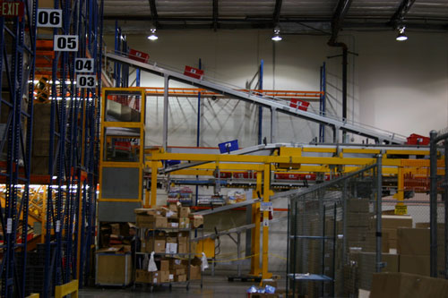 Newegg's operations look very consistent with other warehouses I have visited (random item locations powered by a picking system, pick to light (PTL) conveyors with totes, manual and automatic boxing, etc.), but if you spent time really looking at the detailed processes I bet you might find a few innovative things that give Newegg a competitive advantage. The reason I believe this to be the case is that Newegg runs a very powerful, organized website and many of their products are high value, yet are also low weight. Newegg runs warehouses in CA and TN, so that gives them good access to both the east coast and west coast markets with adequate service to the middle of the country. The article mentions Newegg's target delivery goal twice, and I think it is an admirable one.
"Newegg's goal is to be able to have your shipment to you within 2 days of ordering it regardless of shipping method. It's not a guarantee, but rather an internal goal that they've been striving for ever since their inception. "
"We put great effort into building a bulletproof infrastructure because we are committed to ensuring our customers have the best service. Sure, you can find smaller companies that may be a dollar or so cheaper, but at Newegg we decided we wanted to give our customer the best experience every time, and that is why we must invest into advanced systems that other companies do not have. We built all this with the customer specifically in mind."
Thursday, October 25, 2007
Canon Lens Plant Tour
This Canon plant tour shows all of the steps to create a camera lens from start to finish, and the featured product the EF 500mm F4L IS USM is a gigantic lens at 19.7 inches in length! Also be sure to check out the Lens Gallery at the bottom which has more information about lens materials and physics.
Tuesday, October 23, 2007
SMT Machines Amaze me...
 With coverage on the two Plant tours below (Kingmax and Gigabyte) I thought it was worth sharing more information on Surface-mount technology (SMT) machinery such as the Fuji machine pictured to the right. For high volume products with many components (chips, capacitors, resistors, etc.) SMTs are generally a sound investment, as can be seen by their speed (0.068 Seconds per Component aka 40,000 cph) and precision (Placing Accuracy:+/- 0.0039 in. aka +/-0.1mm). As if the speed and precision weren't enough, surface mount components (SMCs) are generally smaller than their leaded counterparts, so the overall PCB and therefore the entire electronic device can be made smaller.
 In order to utilize Surface mount technology, surface mount components must be purchased. An SMT component is usually smaller than its leaded counterpart because it has no leads or smaller leads. It may have short pins or leads of various styles, flat contacts, a matrix of balls (BGAs), or terminations on the body of the component (passives). The part shown in the picture on the left has 112 pins on it. To do this as a standard DIP, the part would be nearly 7 inches in length! That is just too big. With SMT, this part is a little under 1 square inch.
So on to the videos..... I have never seen a SMT machine operate in person, but I would equate the fastest machines of the bunch as essentially being component gatling guns!
Gigabyte Mainboard Factory
Fuji pick and place
Gigabyte Plant Tour
 Today's Plant tour is of the Gigabyte Nan-Ping Factory in Taiwan. To provide some background, GIGABYTE, which was founded in 1986, has become one of the world's largest motherboard manufacturers. In addition to motherboards, GIGABYTE has further expanded its product portfolio to include graphics cards, notebook and desktop PCs, digital home entertainment appliances, networking servers, and other electronic products.
Gigabyte allowed several sites to provide plant tour coverage, so there is both a short, 2 minute video made by Firing Squad (2006), and detailed virtual tour with commentary from PCStats (2005). The factory assembles both motherboards and graphics cards, and is a great primer for those who have never looked at the detailed steps involved in making today's latest electronics. Many people do not realize that the whole process of manufacturing PCBs and similiar devices is very manual labor intesive, and therefore is almost always performed offshore from the US.
"Without a doubt, motherboards are the most complex and essential part of the
modern PC. Not only do they hold the chipsets that pass data from peripherals,
drives and memory to the processor, they also provide slots and ports for all
your other system components and the circuits through which all data must pass.
Perhaps surprisingly then, motherboards get very little respect in the computing
press as compared to other components. They are perpetually the team player and
not the star of the show, and are generally priced as such.With this in mind, it's surprising to learn the amount of work and machinery involved in manufacturing a single motherboard. We'd vaguely imagined some sort of stamping process where all components are slapped onto the bare board in one step and soldered, before being boxed in a big room full of bored workers. Sure there'd
have to be some testing, but how intense could it be?"

